All about FINFET
Introduction
Recent announcements by other IDMs and foundries of their FinFET roadmaps accelerated the discussion about the opportunities and challenges associated with the use of the FinFET in IP design. It also opened up the discussion about the future of CMOS scaling to 7 nanometers (nm) – a scaling that had too many unpleasant derivatives, including leakage and wide variability, for IP designers, if they were to design with planar bulk CMOS.
FinFET technology alleviated several important challenges associated with continued scaling of planar bulk CMOS. However, other challenges related to lithography such as tolerances associated with double-patterning mask alignment, as well as reliability and performance concerns associated with aging, continued to get more acute with every scaling step.
In this article we will discuss the design opportunities and challenges of the FinFET device and link them to the manufacturing and reliability challenges associated with further scaling.
FinFET, The Device: An IP Designer’s Device of Choice
Due to its many superior attributes, especially in the areas of performance, leakage power, intra-die variability, low voltage operation (translates to lower dynamic power), and significantly lower retention voltage for SRAMs, FinFETs are replacing planar CMOS as the device of choice.
Figures 1 and 2 are simplified depictions of a planar FET and a FinFET respectively. In the planar FET a single gate controls the source-drain channel. Such a gate does not have good electrostatic field control away from the surface of the channel next to the gate, resulting in leakage currents between source and drain even when the gate is off. By contrast, in the FinFET the transistor channel is a thin vertical fin with the gate fully “wrapped” around the channel formed between the source and the drain. The gate of the FinFET can be thought of as a “multiple” gate surrounding the thin channel. Such a multiple gate can fully deplete the channel of carriers. This results in much better electrostatic control of the channel and thus better electrical characteristics.
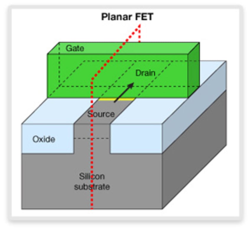
Figure 1: Planar FET
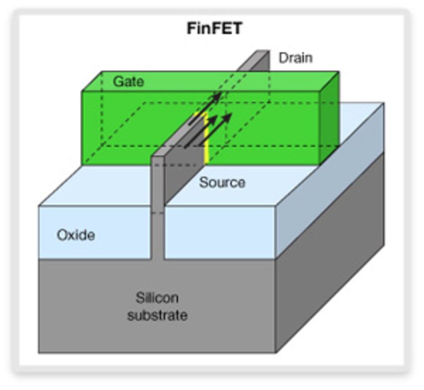
Figure 2: FinFET
The most relevant geometric parameters of a FinFET are its height H, its width (body thickness) Tsi, and its channel length L. Figure 3 illustrates these parameters. The electrical width of a FinFET is twice the height plus the width.
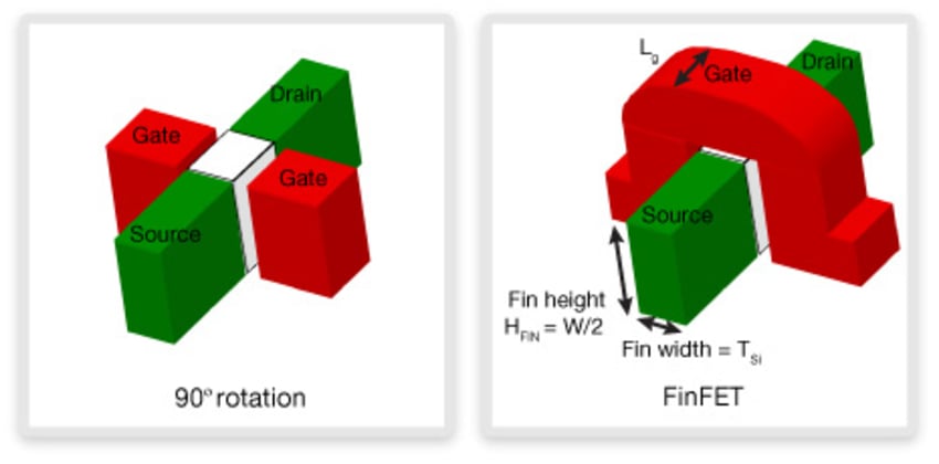
Figure 3: FinFET geometric parameters
At any one technology node the FinFET has several advantages over its planar counterpart including, but not limited to:
Very good electrostatic control of the channel, meaning the channel can be “choked off” more easily. FinFETs boast a near-ideal sub-threshold behavior (associated with leakage), something that’s not easy to achieve in planar technology without considerable effort.
Greatly reduced short channel effects. The short channel effects in planar technology are complex and have a significant impact on gate length variations and, therefore, on electrical performance.
High integration density, 3D, thanks to vertical channel orientation delivers more performance per linear “w” than planar even after the isolation dead-area between the fins is taken into account.
Smaller variability, especially variability resulting from random dopant fluctuation primarily due to doping-free or low doping channels.
FinFET as an Opportunity for IP Design
Design metrics of performance, power, area, cost, and time-to-market (opportunity cost) have not changed since the inception of the IC industry.
Designing in FinFET broadens the design window. Operating voltage continues to scale down, significantly saving on dynamic and static power. Additionally, short channel effects are significantly reduced, decreasing the guard-banding needed to deal with variability, and performance continues to improve (compared to planar at an identical node). In fact, at very low power supply voltages, the performance advantage of the FinFET compared to its planar equivalent widens due to the superior gate control of the channel in the FinFET even at low voltages.
For memory designers, an added advantage of FinFET is the significantly lower retention voltage of FinFET-based SRAM compared to that of planar.
Given the new emerging metric of performance per unit power (Koomey’s law) one major design optimization alternative given the designer in FinFET vis-a-vis planar is greatly improved performance at the same power budget, or an equal performance at a much lower power budget. Quite a good place to be in.
One additional feature that eases the transition from designing in planar to designing in FinFET is the fact that the back-end of the process is essentially the same for both, and therefore a significant amount of the design flow associated with the back-end remains intact.
FinFET Design: The Challenges
FinFET is a significantly more complex device to model. Accurate FinFET parasitic extraction is more complicated. Generating good, yet compact SPICE models is also more challenging than for planar devices. For most design activities the aforementioned complexities are transparent to the designer. However, there still remain many design optimization challenges for the circuit designer utilizing FinFET.
FinFET has a lower DIBL / SS (sub-threshold swing) that is a desirable characteristic as far as leakage is concerned. On the other hand the undoped (or very lightly doped) and practically fully-depleted channel renders the use of body biasing techniques commonly used in planars less effective, making alternatives necessary.
The finite granularity of the fin width “W” and the limited range of freedom in channel length for a given architecture make optimizing analog as well as digital design more complex. Granted that many fins can be “ganged” together to generate a desired “W”, still “L” and “W” are not exactly free continuous parameters. This is because FinFETs are 3D structures, and reining in etch variability for the high-aspect ratio processes with non-uniform pitches or locally varying pitches may be a problem. Thus FinFETs have a significant numbers of restricted design rules (RDR).
For SRAM design, optimizing the β ratio of a bit-cell is more difficult as “W” is quantized, and the flexibility in “L” as a tuning parameter is limited. Practically speaking a β of “1” or “2” are mainly the two available choices. That, in turn, translates to the need for more advanced assist techniques to enhance SRAM yield.
FinFET: Lithography and Manufacturing
Given the fact that EUV will not be ready for volume production anytime soon, the use of double-patterning (DP) is a must for all layers with tight pitches. This is not unique to FinFET. In fact, it applies mostly to interconnect layers (BEOL), which are the same in planar and FinFET technologies.
In the manufacturing of IP, designers are used to digitizing what they plan to build and they are good at modeling and accounting for (simulating) the rounding effects associated with lithography artifacts. At nodes below 22 nm, however, the concept of digitizing a whole active area and then using a “cut-mask” to generate the desired geometry is a direct result of mask alignment challenges associated with double-pattering. It is especially critical to do so for devices where a poor printability does not just result with wide distribution of device parameters, but with totally useless devices. Also, mismatches are intolerable for circuits where transistor matches and layout symmetry is a must such as SRAMs and sense amplifiers.
Figure 4 shows the typical digitization of a 6T-SRAM cell and the corresponding expected print on the silicon under single patterning schemes.

Figure 4: A digitized 6T-SRAM cell and its expected printed image
Figure 5 shows the resulting printed image with double-patterning under horizontal and vertical poly mask misalignment, respectively. Notice that with horizontal misalignment one pair of devices results in a reduced L (fast but very leaky), while the other pair results in a wider L (weak devices). Similarly, for vertical misalignment the mismatch is in W of the devices. Bottom line: you run the risk of having non-functional silicon.

Figure 5: Expected printed image of 6T-SRAM with horizontal and vertical misalignment
Figure 6 shows the scheme of digitizing the contiguous gate layer then using a cut mask to ensure proper printability. Clearly this approach results in the most satisfactory printout for devices. Also, it is noteworthy that this approach of using a “cut mask” is not a FinFET-specific technique and applies to the formation of devices for planar as well as FinFETs beyond 20 nm.

Figure 6: Using cut-mask to generate desired printed image for 6T-SRAM
Patterning and corresponding challenges from an optical proximity correction and multiple double patterning (OPC/MDP) point of view are not expected to be fundamentally different from planar patterning, apart from the fin generation process, which is currently seen as generating a “corrugated substrate.” Spacer patterning is preferential, since the fins are sensitive to thickness variations. Support of DPT coloring and decomposition compliance checking is no different than that of all advanced nodes using DPT.
From a physical layout perspective FinFET design has a disproportionate number of RDRs. Lithography is only one reason for these RDR: the fin patterning/formation process with the high aspect ratio etches and the fragility of the fins under the high stress necessary for mobility enhancements are further factors driving towards high restrictions.
A simplified representation of the process of manufacturing FinFET structures is shown in Figures 7, 8, and 9. The key steps involved are:
The definition of the active device areas is shown as the blue mandrels (temporary supporting structures). The fins (red) are formed by etching the mandrels (Figure 7). Then a cut mask is used to remove the unwanted parts of the structure (Figure 8) leaving the final pattern (Figure 9).
Given that the FinFET technology will be implemented at 20 nm or beyond, double patterning techniques are used. A “spacer double patterning” is usually the preferred technique for pattering the fins.

Figure 7: Mandrels

Figure 8: Cut mask
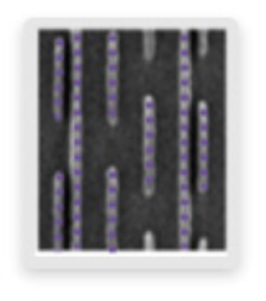
Figure 9: Patterned structures
A FinFET manufacturability rule (to alleviate severe performance consequences) worth mentioning specifically is the rule associated with “lonely” FinFETs.
The dependency of device performance on layout is well understood and modeled in planar CMOS, but in FinFETs, given the 3D nature of the fins, the SiGE stress profile of a P-device loses all effectiveness when the device is not part of a cluster. Therefore, it is necessary to enforce strict dummy device clustering rules to ensure proper performance of active P-type FinFETs.
Figure 10 illustrates the TCAD simulated stress profile of a P type FinFET. It shows the stress degrading from over 1200 MPa (for clustered devices) to almost zero.
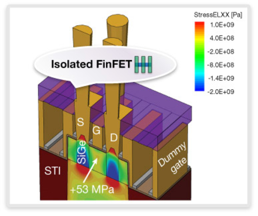
Figure 10: TCAD simulated stress profile of a lonely P FinFET
FinFET: Aging
Aging is related to the physics of the high-K dielectric gate stack and is by no means a FinFET phenomenon, yet FinFET designers have to deal with this reliability concern in the form of simulating and accounting for the effects of Negative Bias Temperature Instability (NBTI) and Positive Bias Temperature Instability (PBTI ) aging that alters the behavior of the device. The industry’s experience (history) in this area is unfortunately limited and it is an added variable to deal with.
NBTI, which impacts P-type devices and PBTI, which impacts N-type devices, are a shift (deterioration) in the threshold of the device, Vt that is a function of VGS, temperature, and time. It is a partially reversible process that depends on the time a device is on and the corresponding duration of recovery (device off). It is highly sensitive to high temperature. Over years of use a device threshold could shift significantly impacting the delay of a critical path by as much as 7% to 10%. NBTI is much more critical than PBTI. NBTI is an order of magnitude higher than PBTI.
Figure 11 shows the typical shift in Vt as a function of time and temperature for an “on” device. Similarly, Figure 12 shows the corresponding gate delay degradation as a function of time and temperature.
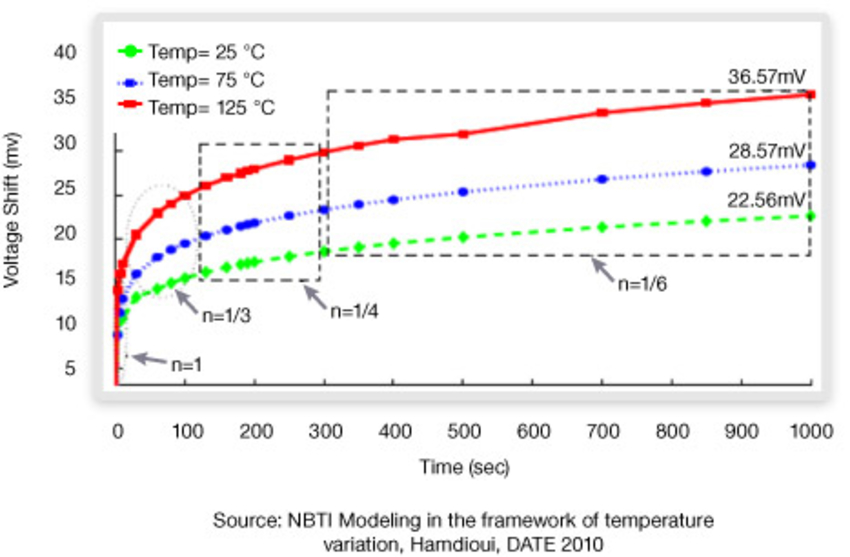
Figure 11: Vt shift as a function of time and temperature
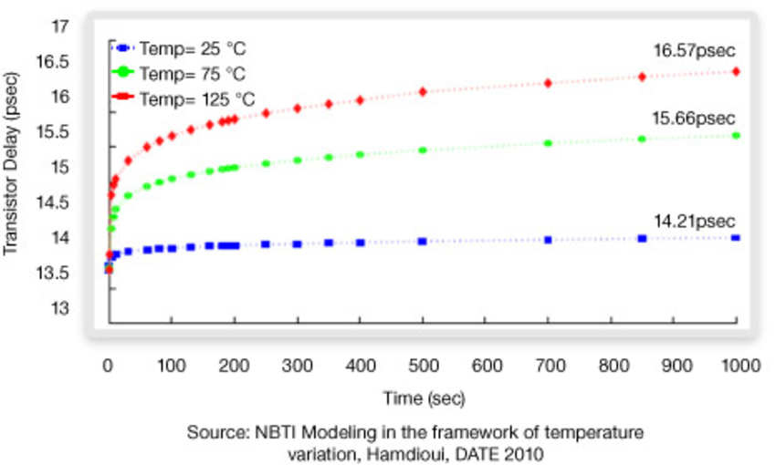
Figure 12: Delay degradation as a function of time and temperature
FinFET: SER
Soft Error Rate (SER) upsets due to impinging particles are an important parameter to monitor, especially for SRAMs. How does SER look as we move from planar to FinFETs? The answer is simply: better.
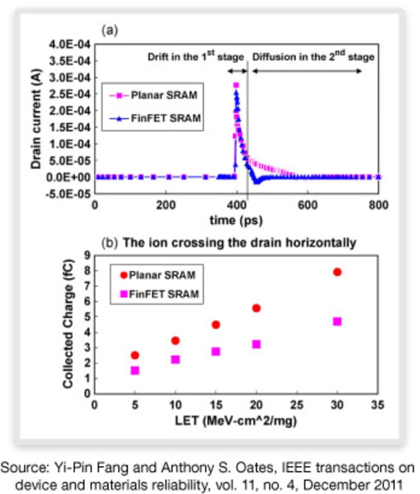
Figure 13: Drain current and collected charge comparison of planar and FinFET for SRAM
Simply explained, charge generation caused by energetic impinging particles is in the substrate. In planar, a lot of it can reach the drain of the device and collect there, causing enough current to upset the storage node. In FinFETs, the conduction is mainly in the channel and, thus most of the charge dissipates in the substrate and will not collect at the drain, making the probability of upset much lower, as the simulated data shown in Figure 13 indicates.
Summary
FinFET is the most promising device technology for extending Moore’s law all the way to 5 nm. It offers excellent solutions to the problems of sub-threshold leakage, poor short-channel electrostatic behavior, and high device parameters variability that plagued planar CMOS as it scaled down to 20 nm. Furthermore, its ability to operate at much lower supply voltage extended voltage scaling which was leveling off and allowed further badly needed static and dynamic power savings.
Comments
Post a Comment